RT9490/RT9492 Application Note: Implement Charge System with the RT9490/RT9492
Jax Li | AN081
The RT9490/RT9492 is a highly integrated 5A Buck-Boost switch mode battery charge management and system power path management device for 2-4 cell Li-Ion and Li-polymer battery. The function settings of RT9490/RT9492 are both hardware pins and software register settings. Charging and system configurations are accessible through I2C serial interface, offering a versatile charging solution. This application note aims to present the most prevalent application and design scenarios for designers’ reference.
1 Framework of Charging System
Figure 1 is a typical framework of a charging system with the RT9490/RT9492. The RT9490/RT9492 can control two AC-RBFET and support dual input applications. In this charging system, an external reverse-blocking MOSFET (AC-RBFET) is placed between the USB connector and the RT9490/RT9492. The second AC-RBFET is an option for another input, such as wireless. The RT9490/RT9492 can also support D+/D- detection to achieve BC1.2 detection and special adaptor detection.
The SYS pin of the RT9490/RT9492 supplies system power. It has automatic power path selection to supply system power from the BUS, battery, or both. For the shipping mode function, an external SHIPFET is placed between the battery and the BAT pin of the RT9490/RT9492. Communication between the host and the device is through I2C serial interface.
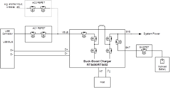
Figure 1. Typical Framework of Charging System
Moreover, for USB Type-C, a PD controller can be used to communicate with the adapter by USB Type-C and Power Delivery (PD) protocol, such as the RT1715. A fuel gauge IC can be used in battery pack to calculate the SOC of the muti-cell battery, such as the RT9440. Figure 2 shows the charging System with a PD Controller.
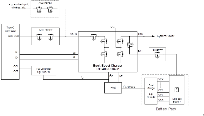
Figure 2. Charging System with PD Controller
2 Charging System Work Procedure
Based on the typical framework of a charging system, the typical work procedure is shown in Figure 3. After the battery is attached to the system, the power path of the RT9490/RT9492 will turn on, powering the system. Following system power-up, the host should initially initialize the RT9490/RT9492 register settings. Once the adapter is plugged into the USB connector, the bus source type is initially identified. Following BC1.2 detection, the host should configure the charge parameters. Subsequently, the RT9490/RT9492 starts charging until the battery reached full capacity or the adapter is unplugged. If the product supports another special charging protocol, the work procedure may follow another pattern as shown in Figure 4. The special charging protocol detection is done either after BC1.2 detection or directly, bypassing BC1.2.
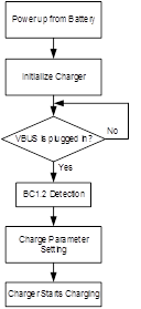
Figure 3. Charging System Work Procedure
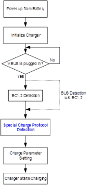
Figure 4. Flow with Special Adaptor Detection
3 Hardware Pin Setting
There are some hardware pins should be determined before the RT9490/RT9492 is powered up.
Figure 5. The RT9492 Typical Application Circuit
3.1 PROG Pin
During power-on reset (POR) stage, the device detects the PROG pin pull-down resistance, and then sets register 0x0A[7:6] for BATTERY_CELL and register 0x13[5] for PWM_FREQ. Refer to Table 1 for the PROG pin pull-down resistor selection. It is recommended that the pull-down resistor on PROG pin to have ±1% to 2% tolerance for its resistance.
Table 1. PROG Pin Resistance for Cell and Frequency Setting
|
Cell
|
Resistance for Typical Value
|
Frequency
|
BATTERY_CELL
|
PWM_FREQ
|
|
2s
|
6.04kW
|
1.5MHz
|
01
|
0
|
|
8.2kW
|
750kHz
|
1
|
|
3s
|
10.5kW
|
1.5MHz
|
10
|
0
|
|
13.7kW
|
750kHz
|
1
|
|
4s
|
17.4kW
|
1.5MHz
|
11
|
0
|
|
27.0kW
|
750kHz
|
1
|
3.2 ACDRV Pin
The charger has two ACDRV drivers to control optional back-to-back N-channel MOSFET for input power source selection. During POR, ACDRV pin detects the presence of optional AC-RBFET and then updates status to ACRB1_STAT and ACRB2_STAT. Table 2 shows the detailed status.
Table 2. Optional AC-RBFET Status for Input Power Selection
|
Scenario
|
ACDRV1 Pin
|
ACDRV2 Pin
|
REG 0x1E [6]
ACRB1_STAT
|
REG 0x1E [7]
ACRB2_STAT
|
|
No AC-RBFET is used
|
Shorted to GND
|
Shorted to GND
|
0
|
0
|
|
AC1 RBFET is used
|
Connected to AC1 RBFET Gate
|
Shorted to GND
|
1
|
0
|
|
AC2 RBFET is used
|
Shorted to GND
|
Connected to AC2 RBFET Gate
|
0
|
1
|
|
AC1 and AC2 RBFET are used
|
Connected to AC1 RBFET Gate
|
Connected to AC2 RBFET Gate
|
1
|
1
|
3.3 SDRV Pin
The RT9490/RT9492 supports SDRV driver for the optional SHIPFET. The SDRV is connected to the external ship FET, and it remains turned off in ship or shutdown mode. If a ship FET is not used, a 1nF/50V capacitor must be connected from SDRV to GND.
With the optional SHIPFET, following POR, the register SHIP_FET_PRESENT must set to 1 by the host, and the SHIPFET is controlled by the register SDRV_CTRL.
3.4 ILIM_HZ Pin
This pin is for input current limit setting and HZ mode control. Use a resistor divider to divide the REGN voltage and connect it to the ILIM_HZ pin. The pin voltage is calculated as VILIM_HZ = 1V + 800mW x ILIM, where ILIM is the target input current limit. The input current limit for charger is determined by the lower setting between ILIM_HZ and AICR register. When the pin voltage falls below 0.75V, the buck-boost converter stops switching and REGN on. Conversely, when the pin voltage exceeds 1V, the converter resumes switching.
3.5 CE Pin
Charge enable pin. Active low. When this pin is driven low and CHG_EN = 1, battery charging is enabled. It is important not to leave this pin floating.
If the system does not need to control the RT9490/RT9492 charge via a hardware signal, simply pull this pin to low.
4 Charger Control Flow
To implement the RT9490/RT9492 in a system, a typical device control flow example is shown in Figure 6.
Figure 6. The RT9490/RT9492 Implementing Control Flow
4.1 Power-On Reset
Normally, when the battery is initially attached to the system, the device powers internal bias circuits from the VBATP and VBAT. In another case, only the adapter is plugged into the system. In this case, the device powers internal bias circuits from the VAC1/VAC2 and VBUS. When VBATP rises above VBATP_UVLO, VBAT rises above VBAT_UVLO, VAC1/VAC2 rises above VAC_UVLO, and VBUS rises above VBUS_UVLO, the I2C interface is ready for communication and all the registers are reset to their default value.
4.2 Charger Initial Setting
After the system POR, the host should initialize the register setting of the RT9490/RT9492. It is recommended to initialize the following registers in the beginning.
1. BATTERY_CELL
2. WATCHDOG
3. VSYSMIN
4. VBAT_REG
5. ICHG_CTRL
6. VMIVR
7. AICR
8. VPRE_CHG
9. IPRE_CHG
10. IEOC
11. VRECHG
12. EN_CHG
13. EN_TE
14. VAC_OVP
15. PWM_FREQ
16. SHIP_FET_PRESENT
17. ILIM_HZ_EN
18. JEITA_DIS
19. BC12_EN
20. BC12_EN_CHANNEL
21. DCDT_SEL
22. AUTO_AICR
23. AUTO_MIVR
4.3 REG 0x0A BATTERY_CELL
It should be notice that when the host needs to program any parameter in REG 0x0A, the host must program REG0x0A first, then the host can program other registers. This is because setting BATTERY_CELL will reset VSYSMIN/VBAT_REG/ICHG_CTRL.
4.4 VSYSMIN
This is the minimum system operating voltage. While the adapter is present and the battery voltage is below the VSYSMIN setting, the BATFET operates in saturation mode as an LDO, and the system voltage typically remains 200mV above the VSYSMIN setting. Set VSYSMIN according to the system design, ensuring it is set below VBAT_REG.
4.5 VBAT_REG
VBAT_REG is the fully charged level of the battery. Set this level according to the battery specification initially to avoid overcharging.
4.6 ICHG_CTRL
This is the fast-charging current value. Set this value according to the battery specification initially to avoid exceeding the specification.
4.7 AICR and ILIM_HZ_EN
The input current limit for the charger is determined by lower setting between the ILIM_HZ and AICR registers. If the host wants to set the input current limit value higher than ILIM_HZ value, it should disable ILIM_HZ_EN to deactivate the hardware pin current limit function.
4.8 EN_CHG
Charging of the battery can only commence when the CE pin is set low and CHG_EN = 1. Initialize this register to specify whether the charger can automatically begin charging after the adapter is connected or not. If the system requires waiting for the charging algorithm, set CHG_EN = 0 initially.
4.9 SHIP_FET_PRESENT
The device supports SDRV driver for optional SHIPFET. With optional SHIPFET, after POR, the register SHIP_FET_PRESENT must set to 1 by the host, and the SHIPFET is controlled by the register SDRV_CTRL.
4.10 MASK
The IRQ events in register 0x28 to 0x2D are unmasked by default, while those in register 0x4D are masked by default. The device only reports unmasked IRQ events to the host by the INT pin. Make sure that the required function flags are unmasked.
4.11 BC12_EN
BC1.2 detection function is enabled in default setting. It will automatically detect BC1.2 after adaptor is plugged in. Determine whether use the RT9490/RT9492 BC1.2 function and do BC1.2 flow first.
4.12 BC12_EN_CHANNEL and DCDT_SEL
If use the RT9490/RT9492 BC1.2 function, select the BC1.2 detecting USB port by setting BC12_EN_CHANNEL to VAC1 or VAC2. Set DCDT_SEL to select the BC1.2 data contact behavior.
4.13 AUTO_AICR
When the register AUTO_AICR is set to 1, the device automatically adjusts the AICR after detecting the VBUS source type. Determine whether to use the RT9490/RT9492 auto AICR function. If AUTO_AICR = 1, AICR setting result is listed in Table 3. The AICR register is then automatically changed to the detection result of VBUS_STAT.
Table 3. AICR Setting from D+/D- Detection
|
Detection
|
AICR Setting
|
VBUS_STAT
|
|
USB SDP
|
0.5A
|
0001
|
|
USB CDP
|
1.5A
|
0010
|
|
USB DCP
|
3.25A
|
0011
|
|
NSDP
|
3.25A
|
0101
|
|
Special Adapter
|
1A/2A/2.1A/2.4A
|
0110
|
4.14 Interrupt Event Detection
Whenever IRQ events occur, the INT pin generates a pulse low with 256ms to inform the host. The host should check the Flag and the STAT. According to the event, the host executes the relative action.
4.15 Plug-In BUS Source Type Detection
After the adaptor is plugged in, the RT9490/RT9492 will generates an IRQ on the INT pin. In the case BC12_EN_CHANNEL = 0 (VAC1), an adaptor plug-in event is considered true if the VAC1_PG_FLAG = 1 and VAC1_PG_STAT = 1, as shown in Figure 6.
Once the adaptor plug-in event occurs, the host can proceed to use the RT9490/RT9492 for BC1.2 detection. The host sets BC12_EN = 1 or allow the RT9490/RT9492 to automatically detect the port if BC12_EN is already enabled at the initial stage.
After the RT9490/RT9492 completes BC1.2 detection, the INT pin generates an IRQ to inform the host. The host should check whether BC1.2_DONE_FLAG = 1 and BC12_DONE_STAT = 1. If BC1.2_DONE_FLAG = 1 and BC12_DONE_STAT = 1, then the host can check the 0x1C VBUS_STAT to get the bus source type information.
If the system supports special charging protocol, the host can also proceed to go the special charging protocol detection after BC1.2.
4.16 Charge Parameter Setting
After the host know the type of the input source, according to it the host should set the appropriate charge parameters for the system and BUS source. Such as ICHG_CTRL, VMIVR, AICR, EN_CHG, etc.
Once EN_CHG = 1, the RT9490/RT9492 Starts to charge battery.
If EN_TE = 1, the RT9490/RT9492 will terminate charging at the end of charge stage (When the battery voltage is above recharge threshold, and the charge current is below IEOC_CHG). The RT9490/RT9492 will start to charge again when battery voltage is under recharge voltage threshold
If EN_TE = 0, the RT9490/RT9492 will continue charging at the end of charge stage.
4.17 BUS Plug-Out Event
If the BUS is plugged out, the RT9490/RT9492 will stop charging and send the IRQ event. In the case where BC12_EN_CHANNEL = 0 (VAC1), an adaptor plug-out event is considered true if the VAC1_PG_FLAG = 1 and VAC1_PG_STAT = 0.
The host can reset the charge parameters and hardware control pin after plug-out event.
5 ADC Function
Operation
The ADC is enabled when ADC_EN = 1. Set ADC_CONV_CTRL for One shot mode or Continuous mode. All the ADC channels can be enabled or disabled in the register 0x2F and 0x30. The default settings are enabled.
After power-on reset (POR), when ADC_EN = 1, the ADC results are updated to the register for each channel after ADC conversion. Figure 7 shows the ADC usage example in continuous mode. The typical ADC conversion time is around 3.6ms for each ADC channel. Please refer to the datasheet specifications. In the continuous mode, the host should wait for the ADC conversion time before polling ADC value.
Notice that the quiescent current will increase while ADC is enabled. Please refer to the specifications in the datasheet. This should be considered when the system is in battery-only mode, or when the input bus current ability is limited.
Figure 7. ADC Continuous mode operating flow
In one-shot mode, once the ADC conversion is completed, an INT pulse is generated to notify the host. The host should check whether ADC_DONE_FLAG = 1 and ADC_DONE_STAT = 1, as shown in Figure 8. After the ADC conversion is completed, the ADC_EN will be automatically reset to 0 in one-shot mode. The host should set ADC_EN = 1 again if it needs to get a new ADC value next time. In addition to using interrupts, the host can also achieve one-shot mode ADC reading by polling ADC_DONE_FLAG and ADC_DONE_STAT as shown in Figure 8.
Figure 8. ADC One shot mode operating flow
6 OTG Control
Flow
The RT9490/RT9492 supports OTG (On-The-Go) mode and enters OTG mode via register EN_OTG. The maximum output current is up to 3.32A. In OTG mode, output voltage (VOTG), output current limit (IOTG) and input current limit (IBAT_REG) can be programmed by the host. The OTG mode operation is shown in the Figure 9.
The OTG mode can be enabled under the following condition:
1. VBAT is above VOTG_LBP rising threshold.
2. EN_OTG is set to high.
3. If JEITA function is enabled, voltage at the TS pin should be within acceptable range (VVTS_HOT_OTG < VTS < VVTS_COLD_OTG).
Before the host enable OTG mode, it should set the RT9490/RT9492 register setting first. It is recommended to initialize below registers.
1. VOTG
2. IOTG
3. DIS_OTG_OOA
4. DIS_VOTG_UVP_HICCUP
5. IBAT_REG
6. OTG_HOT and OTG_COLD
Subsequently, when the system detects that the sink device is plugged in, the host should determine the VOTG and the IOTG for the sink device. After configuring the relative registers of OTG mode, the host can enable the EN_OTG if there are no faults. If the system uses the ACDRV function of the RT9490/RT9492 to control the external AC-RBFET, the host should also enable the output channel at the same time while enabling EN_OTG. For example, if only the ACDRV1 is used, the EN_ACDRV1 should be set to 1 after EN_OTG = 1. The other scenario settings are detailed in the datasheet.
After OTG mode is successfully activated, an MIVR IRQ event is generated to notify the host and VBUS_STAT will indicate 0111(OTG mode).
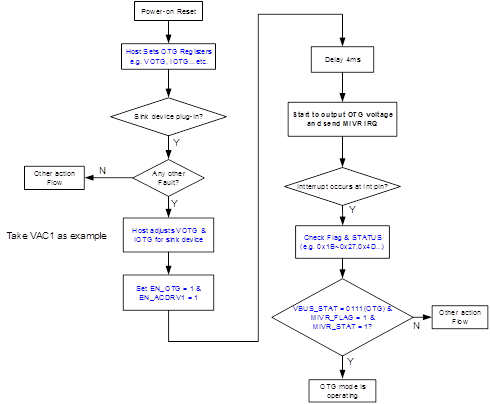
Figure 9. OTG Mode Control Flow
The RT9490/RT9492 OTG mode can also achieve Fast Role Swap (FRS), seamless, and DP/DM HOST mode. The implementing details are described in the datasheet.
7 Shipping Mode Control Flow
The RT9490/RT9492 supports the shipping mode to extend battery life during shipping or storage. This function is realized by the external SHIPFET. To activate the shipping mode, use the SHIPFET and set SHIP_FET_PRESENT to 1. When operating in battery-only condition, set SDRV_CTRL to 10 (Ship mode) and the device will enter Ship Mode as Figure 10. When the device enters ship mode, the device deactivates SHIPFET and internal BATFET.
The device can exit Ship Mode to restore power to the system, using following method:
1. VBUS plugged in
2. Set SDRV_CTRL to IDLE
3. Set RST_ALL or REG_RST bit to reset all registers to default
4. Press the QON pin from high to low.
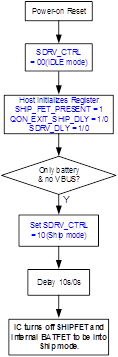
Figure 10. Ship Mode Control Flow
7.1 Shutdown Mode
In addition to ship mode, the RT9490/RT9492 supports extremely minimal battery leakage current with shutdown mode. When the device enters Shutdown Mode, it deactivates the SHIPFET, internal BATFET and circuit. The only way for device to exit shutdown mode and restore power to the system is by plugging in VBUS, and all registers return to their default settings when the device exits shutdown mode. When operating in battery only condition, the device can enter shutdown mode.
The setting method is almost identical to the ship mode as shown in Figure 11. The difference is that SDRV_CTRL should be set to 01 (Shutdown mode).
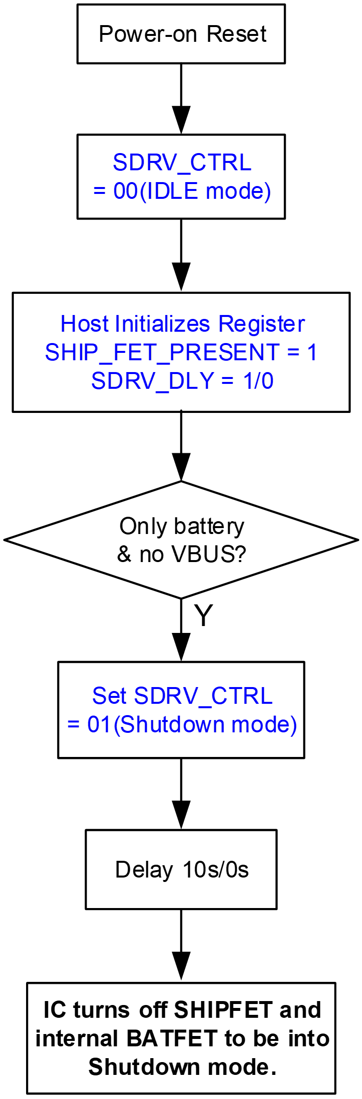
Figure 11. Shutdown Mode Control Flow
8 DP DM Manual Mode
The device supports manual control mode for DP/DM output by programmed DP_CTRL/DM_CTRL. The settable voltage is listed in Table 4. This function can be used to program the DP/DM voltage level, enabling communication or control the adaptor with a special charging protocol as shown in Figure 4.
Table 4. DP_CTRL/DM_CTRL Setting Value
|
Bit Name
|
Description
|
|
REG 0x47[7:5] DP_CTRL
|
000: HIZ (Default)
001: 0V
010: 0.6V
011: 1.2V
100: 2.0V
101: 2.7V
110: 3.3V
111: Reserved
|
|
REG 0x47[4:2 DM_CTRL
|
When using this function, the EN_HZ also must be set to 0. After setting DP_CTRL/DM_CTRL voltage, the REGN will activate, and the manual control output voltage will be provided on DP/DM.
If BC12_EN =1 initially, when the adapter is plugged in, the device will ignore manual control settings during BC1.2 detection. Once BC1.2 is completed, an INT signal is asserted to the host to indicate BC1.2_DONE and DPDM_DONE, and then the manual control will be enabled.
9 Conclusion
This application note introduces how to implement a charge system with the RT9490/RT9492. Firstly, it presents the framework of a typical charging system. In the subsequent section, this note explains the basic operating procedure of the system. Based on this procedure, it provides an example of the device control flow for design reference. In addition, this note delves into the usage of the ADC function, the OTG mode, the ship mode and the DP/DM manual mode.
This encompasses all the content covered in this application note. To stay updated with more information about our products, please subscribe to our newsletter.